Photonic Crystal (PCS)
Photonic Crystal (PCS)
Photonic Crystal is a nanoscale periodic structure designed to control the flow of light (photons) in a way similar to how an ordered crystal controls the flow of electrons in a semiconductor. It consists of periodic structures that produce a photonic energy gap, within which light cannot propagate at certain frequencies, just as with energy bands in crystals in the electron context.
The following are some basic concepts of Photonic Crystals:
- Photonic BandgapOne of the most important features of photonic crystals is their ability to create an energy gap, that is, a range of frequencies in which the propagation of light (photons) is forbidden. This is similar to the energy gap in crystals in the electron context, where electrons cannot occupy certain energy levels within a given range.
- Light GuidancePhotonic crystals can function as light guides, allowing control of light flow and concentration of light at a very small scale. This enables applications in photonic devices such as lasers, modulators, and photodetectors.
- Dispersion ControlPhotonic crystals allow control of light dispersion, which can be used to produce unique optical properties such as negative dispersion, in which light with a shorter wavelength has a higher phase velocity than light with a longer wavelength.
- ApplicationsPhotonic crystals have various applications in the field of photonic technology, including optical communication, optical signal processing, optical sensors, and other optoelectronic devices.
Photonic crystals have been the subject of extensive research in optics and photonics because of their potential to bring major advances in photonic devices and applications in the future.
Applications of Photonic Crystals are very diverse and continue to grow with advances in the understanding and technology of photonic crystals. The following are some of the main applications:
- Integrated Optical DevicesOne of the main applications of photonic crystals is in integrated optical devices. Photonic crystals can be used to create microstructures that guide, manipulate, and focus light with high precision. This is useful in developing integrated optical circuits for optical communication, information processing, and optical computing.
- Photodetectors and Optical SensorsPhotodetectors and optical sensors use photonic crystal principles to improve sensitivity and responsivity. Photonic crystals can be used to improve light collection efficiency and increase light detection sensitivity across various wavelength ranges.
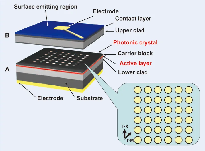
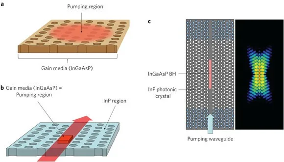
- Photonic Crystal LasersPhotonic crystals can be used in laser design to produce unique optical properties, such as controlled mode distribution, single-mode lasing, and high efficiency. This opens the door to developing smaller, more efficient, and more advanced lasers for various applications such as optical communication, medicine, and material processing.
- Optical Filters and DemultiplexersPhotonic crystals can be used to create highly selective optical filters and demultiplexers that separate optical signals into different frequency channels. This is useful in optical communication systems that require precise and efficient separation of light channels.
- Micro Light GuidesPhotonic crystals can also be used as micro light guides, which allow control of light flow within microscopic structures. This can be exploited in devices such as integrated optical waveguides, optical interferometers, and other micro-optical components.
- Optical MetamaterialsPhotonic crystals are often used in the development of optical metamaterials, which are artificial materials with optical properties not found in natural materials. Optical metamaterials have the potential to produce negative refractive index effects, super-resolution focusing, and unique light reflection.
These are just a few examples of the many potential applications of photonic crystals. As research continues, new and innovative applications are expected to emerge in various fields of photonic technology.
